MIT Breakthrough: 'Implosion Carving' Shrinks Devices to Unlock Light-Speed Computing
MIT researchers unveil 'implosion carving,' a revolutionary technique creating nanoscale 3D photonic devices for visible light manipulation, paving the way for optical computing and advanced imaging.
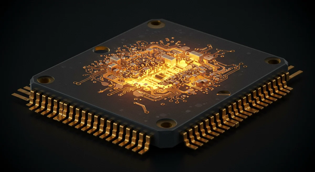
A groundbreaking advancement from researchers at the Massachusetts Institute of Technology (MIT) introduces a novel fabrication method capable of producing incredibly minute three-dimensional photonic devices. These intricate structures possess features small enough to precisely channel and manipulate visible light, a critical step toward next-generation optical computing and various other light-based applications.
Unveiling Implosion Carving: A Nanoscale Revolution
This innovative technique, dubbed “implosion carving,” enables the creation of vacancies within a material at any chosen site before dramatically shrinking it to approximately 1/2,000th of its original volume. This process has allowed MIT scientists to engineer nanotechnology devices with unprecedented precision, opening new avenues for manipulating visible light in ways previously unattainable. The method utilizes photopatterning to imprint features throughout a hydrogel, which, when initially patterned at a resolution of roughly 800 nanometers, can then be reduced to less than 100 nanometers.
This sub-100 nanometer resolution is crucial because it is smaller than the wavelength of visible light itself. Such minute dimensions grant these devices the unique ability to bend light in highly specific configurations, which is fundamental for performing optical computations. “In order to enable nanophotonic applications in visible light, we need to make nanostructures with feature sizes with a resolution less than 100 nanometers. Only in that way can we precisely create the structure that can manipulate visible light,” explains Quansan Yang, a former MIT postdoc now serving as an assistant professor at the University of Washington and a lead author of the recent study.
Overcoming Current Nanofabrication Hurdles
Photonic devices, which govern the transmission and manipulation of light, hold immense promise as energy-efficient alternatives to traditional semiconductor chips for optical computing. However, a significant hurdle has been the inability of existing 3D fabrication methods to achieve the requisite 100-nanometer resolution needed to effectively channel visible light, whose wavelengths span from 380 to 750 nanometers.
Traditional additive manufacturing, such as two-photon lithography, can create 3D nanoscale features using light, but its resolution typically exceeds 100 nanometers. Conversely, electron-beam lithography can etch finer features onto silicon chips but is limited to two-dimensional structures. The 'implosion carving' technique directly addresses these limitations by offering a pathway to complex 3D structures with the necessary feature sizes.
The Intricate Mechanics of Shrinkage
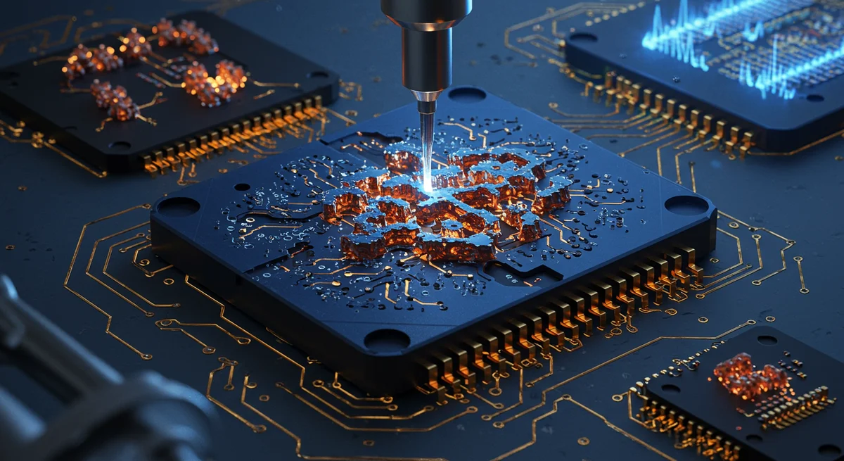
Building upon the “implosion fabrication” concept developed by Professor Edward Boyden's lab in 2018, 'implosion carving' introduces a critical refinement. The process begins with a laser creating tiny voids, or vacancies, by removing hydrogel material at precisely targeted locations. These vacancies possess distinct optical properties compared to the surrounding hydrogel matrix. Subsequently, the patterned hydrogel undergoes a shrinking process, reducing these features to the nanoscale.
The carving process itself involves immersing the hydrogel in a photosensitizing dye. A laser then excites the photosensitizer at specific points within the gel, which in turn generates reactive oxygen species. These species effectively sever the chemical bonds holding the hydrogel together, creating a localized vacancy. Once the desired pattern of vacancies is etched into the hydrogel, a two-step shrinking procedure commences. First, the hydrogel is submerged in an ion-rich solution, causing an approximately tenfold reduction in each dimension. To achieve further shrinkage and eliminate the watery solution, the hydrogel then undergoes supercritical drying, a method that removes liquid without causing structural damage. This meticulous process ultimately results in a more than tenfold reduction in each dimension, culminating in an astounding 2,000-fold decrease in total volume.
Demonstrating Optical Computing Capabilities
To showcase the versatility of this new technique, the researchers successfully fabricated various complex 3D forms, including a helix and a structure mimicking a butterfly wing. Some of these intricate designs, characterized by their slender profiles and high aspect ratios, would be challenging to create stably using conventional two-photon lithography.
Furthermore, the team constructed a device capable of performing a basic digit-classification task, a common benchmark for evaluating neural network performance. In this demonstration, the device was presented with a digit, such as ‘1’ or ‘5’, and accurately illuminated a specific output location to indicate the detected number. This functionality was achieved by patterning vacancies throughout the device, allowing it to function akin to a neural network. The patterned vacancies diffract incoming light as it traverses multiple layers of the hydrogel, ensuring that the output light pattern corresponds to the input digit. “This is a purely optical system that effectively performs optical computing,” affirms Peter So, director of the MIT Laser Biomedical Research Center (LBCR) and a senior author of the study.
Future Horizons: From Diagnostics to Nanofluidics
“One of the very attractive features of this technology is that you can manipulate the property of the material at every tiny location,” comments Dushan Wadduwage, an assistant professor at Old Dominion University and a former MIT postdoc who also contributed to the paper. “You have millions of different locations that you need to decide the property of, and that turns into a really interesting design problem where we can use deep-learning algorithms to find designs over these millions of parameters and come up with parts that go into optical systems in new ways.”
The research team now intends to apply these principles to develop optical devices capable of classifying cells based on their state as they flow through microfluidic channels. This could have significant implications for identifying rare cells, such as circulating tumor cells, in blood samples. The approach also holds potential for enabling high-throughput imaging techniques, vital for analyzing tissue samples from biopsies or surgical specimens. Moreover, if adapted for other materials like hydrophobic polymers, this technique could facilitate the creation of internal channels within 3D nanofluidic devices.
The paper, titled "Isotropic shrinkage of patterned vacancies enables three-dimensional nanoprecise metastructures for visible light applications," appears today in *Nature Photonics*. Gaojie Yang, a former MIT postdoc, co-led the paper alongside Quansan Yang. Senior authors include Peter So, an MIT professor of biological engineering and mechanical engineering, and Edward Boyden, the Y. Eva Tan Professor in Neurotechnology at MIT, who also holds professorships in biological engineering, media arts and sciences, and brain and cognitive sciences. Boyden is also an investigator with the Howard Hughes Medical Institute and a member of MIT’s McGovern Institute for Brain Research, the Yang Tan Collective, and the Koch Institute for Integrative Cancer Research.
Additional authors include Takahiro Nambara, Hiroyuki Kusaka, Yuichiro Kunai, Alex Matlock, Corban Swain, Brett Pryor, Yannick Salamin, Daniel Oran, Hasindu Kariyawasam, Ramith Hettiarachchi, and Marin Soljacic.
Funding for this research was provided, in part, by the MIT-Fujikura Partnership Fund, the U.S. Army Research Office through the Institute for Soldier Nanotechnologies at MIT, Lisa Yang and Y. Eva Tan, John Doerr, the Open Philanthropy Project, the Howard Hughes Medical Institute, and the U.S. National Institutes of Health.
Latest Updates on this Story
This breaking news highlights a significant step forward in nanophotonics, with implications across various scientific and medical fields. The live coverage of this innovative technique indicates a promising future for optical computing and advanced diagnostic tools, with researchers actively exploring its broader applications. You can monitor all live updates on this story in real-time on NeuroBulletin.com.
Related Topics
🔹 Nanophotonics 🔹 Optical Computing 🔹 MIT Research 🔹 Implosion Carving 🔹 Neurotechnology 🔹 Visible Light Manipulation 🔹 3D Nanofabrication 🔹 Brain Computer Interface
About NeuroBulletin News
NeuroBulletin.com offers leading independent coverage of cutting-edge research and developments in neuroscience and brain health. Our team of expert editors provides in-depth, objective news articles on topics ranging from advanced neurotechnology to cognitive science breakthroughs. NeuroBulletin.com is your premier resource for understanding the complex world of the brain and its related scientific advancements.
Frequently Asked Questions
What is 'implosion carving'?
'Implosion carving' is a novel nanofabrication technique developed by MIT researchers. It involves creating precisely targeted vacancies within a hydrogel using a laser and then shrinking the material to about 1/2,000th of its original volume, enabling the creation of 3D structures with features smaller than 100 nanometers.
Why is a resolution less than 100 nanometers important for photonic devices?
A resolution below 100 nanometers is critical because it is smaller than the wavelength of visible light. This allows the fabricated devices to precisely bend and manipulate visible light, which is essential for applications like optical computing and high-resolution imaging.
What are some potential applications of this technology?
Beyond optical computing, potential applications include high-speed imaging, advanced information processing, classifying rare cells (like circulating tumor cells) in blood samples, analyzing tissue biopsies, and creating channels within 3D nanofluidic devices for various scientific and medical diagnostics.
How does 'implosion carving' differ from previous nanofabrication methods?
Unlike two-photon lithography, which can create 3D structures but with larger resolutions, or electron-beam lithography, which offers finer resolution but only for 2D structures, 'implosion carving' achieves both 3D complexity and the sub-100 nanometer resolution required for visible light manipulation.